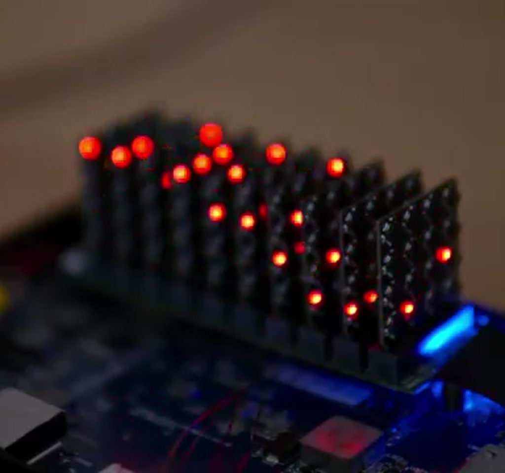
At first glance the board looks like a mistake. Its proportions feel wrong, the component density is unsettling, and nothing about it has the tidy symmetry of consumer hardware. Up close it reads as intent: a hand-built 160-core RISC-V supercluster assembled through iteration, improvisation, and a tolerance for repeated failure.
The real significance here is not the headline core count. What changes how this project should be understood is the interaction between analog limits and scale.
Multiply modest design choices across dozens or hundreds of nodes and small imperfections stop being nuisances and become system-defining.
That observation surfaces immediately: a cluster is not simply many processors glued together. It is a network of power rails, protection diodes, pull-up resistors, connector parasitics, and human decisions.
The project makes plain the lesson most people misunderstand, which is that digital scale often fails for analog reasons.
Because it was built outside an industrial line every compromise left a visible trace. The creator moved from a 206-core attempt to this 160-core design, swapping fragile surface-mount pin headers for higher-density M.2 style edge connectors, and embracing a modular architecture of ten vertical slots.
Each module was a tiny 4-layer PCB, about 22 by 26 millimeters, carrying roughly 64 components, 515 pads, and 413 vias. Those numbers matter because they force specific manufacturing and assembly tradeoffs.
What becomes obvious when you look closer is how dominated the work is by physical thresholds. Trace width, via density, and connector sourcing are not abstract engineering choices; they are financial and logistical constraints that determine what a small project can attempt.
From Concept To Physical Constraint
What becomes obvious when you look closer is how dominated the work is by physical thresholds. Trace width, via density, and connector sourcing are not abstract engineering choices; they are financial and logistical constraints that determine what a small project can attempt.
M.2 Edge Connectors And The Cost Of Scale
M.2 style edge connectors brought higher density and a cleaner mechanical profile compared to the earlier pin headers, but they introduced new procurement headaches.
Many of those connectors were only available in full production reels. That means a one-off decision can require a purchase sized for mass manufacture, converting a small design choice into a disproportionate expense.
There is a clear tradeoff: pay for full production quantities and preserve a tidy assembly flow, or economize on parts and accept time-consuming manual soldering of hundreds of pins. The latter reduces upfront cash outlay but increases assembly labor and introduces human variability into the build quality.
Modularity, Tolerances, And Cascading Complexity
The board’s modular approach, ten vertical slots each hosting a multi‑MCU module, was intended to enable experimentation without redesigning the whole motherboard. In practice the choice multiplied mechanical tolerances and routing challenges. Each connector adds parasitic capacitance and mechanical variability that must be absorbed by the system.
That is a recurring pattern: a design choice that simplifies iteration at one scale creates new boundaries at another. The modular idea works up to the point where alignment, solder quality, and interconnect impedance begin to dominate behavior.
Electronics Under Pressure
Electrical design challenges proved the most revealing. With hundreds of devices sharing power and signals, subtle conduction paths and parasitic effects turned reasonable assumptions into failure modes. Low-side switching for individual MCU programming, for example, looked attractive until hidden current paths inside microcontrollers caused unexpected heating and erratic behavior.
Power Distribution And Brownouts
LEDs intended as trivial indicators became a system-level hazard. Lighting many LEDs at once produced voltage droop and brownout conditions because hair-thin traces and distribution geometry could not sustain the transient currents. Switching LED pins from push-pull to using internal pull-ups reduced current dramatically and stopped the brownouts.
That is a concrete constraint: the cluster’s power profile is bounded by trace thermal limits and total connector current. Each MCU drew about 7 milliamps at 3.3 volts during certain workloads, which is roughly 23 milliwatts per core.
Multiply that by 160 cores, and the system sits in the range of under 4 watts total under typical hashing loads. That figure both motivates the design and defines the power tradeoffs.
Power scaling here is not linear. A single LED change or a 1 millimeter longer trace can shift the thermal and voltage stability of an entire module.
Shared Bus And Signal Integrity
Communication used an open-drain shared bus so many microcontrollers could coexist without destructive drive conflicts. That safety came with an analog cost. Open drain lines rely on pull-up resistors, line capacitance, and timing to form clean transitions. With the chosen 10-kilohm pull-ups, the bus rose slowly, and low-to-high transitions became a source of data corruption at higher frequencies.
Attempting to strengthen pull-ups to 1 kilohm improved rise times but created excessive current loads during certain states and overstressed some devices.
The eventual practical solution was a timing compromise: accept slower throughput and add host-side delays to allow signals to settle. This illustrates a familiar bounded tradeoff: raw speed versus robustness and power budget.
Assembly As An Engineering Process
Hand assembly at this density is unforgiving. Many solder joints are hidden once connectors are installed, which reduces options for inspection and rework. Conventional tools can only go so far. The builder developed improvised techniques, trading elegant methods for stubborn persistence.
Assembly realities included soldering hundreds of connector pins by hand, replacing automated pick and place. That is a time cost constraint measured in hours per module, not in dollars per unit. It also raises repairability concerns because a single imperfect joint can render a module unresponsive and difficult to access.
Programming Strategies And Practical Hacks
Programming the cluster required more than flashing chips one by one. A failed low-side power switching strategy led to unexpected current flow through shared bus and reset lines. The workaround was to connect all grounds and to program all MCUs simultaneously while pre-indexing each MCU to its physical slot. On the hardware side this required repurposing GPIO pins and reassigning roles between the programmer board and the cluster board.
Those are pragmatic editorial choices. The maker traded neat separation of roles for immediate functionality. The decision worked, but it tightened the envelope for future firmware and debugging because interfaces did not match the original intent.
Software, Benchmarks, And Where Parallelism Actually Helps
To show the cluster’s capability the creator implemented a Raymarcher and a SHA256 hashing benchmark. The Raymarcher revealed how communication overhead kills perceived speed. The serial link used for host to cluster messaging operated at 115 kilobits per second. While the interface chip theoretically supports up to 8 megabits per second that throughput had not been achieved in this setup.
The result is a familiar distributed systems constraint: adding compute nodes does not increase end-to-end performance if the interface cannot feed them fast enough. The Raymarcher workload was limited more by serial bandwidth and protocol overhead than by the aggregate instruction rate of the 160 cores.
By contrast the SHA256 hashing workload, which is compute-heavy and low bandwidth, showed the cluster’s strengths. In that specific case the 160 modest cores outperformed an eight-core desktop CPU on raw hashing throughput while drawing under 4 watts. This is a sharp reminder that performance is multidimensional and workloads determine which architecture wins.
Two Concrete Tradeoffs Worth Noting
Tradeoff one: procurement versus labor. Choosing edge connectors with industrial style packaging reduced board footprint but forced either large quantity purchases or painstaking manual assembly. The economic boundary here is a real decision point: a small team can absorb hours of soldering, or they can finance reels of connectors sized for manufacturers.
Tradeoff two: speed versus stability. The shared open drain bus design demanded that pull-up strength, line capacitance, and timing be balanced.
Using 10 kilohm pull-ups kept currents low but required slower signaling and host-side delays. Moving to 1 kilohm would speed transitions but at the cost of higher currents that some devices could not tolerate. That tradeoff is measurable in milliseconds of latency and milliamps of current per line.
Both tradeoffs come with quantified context: the serial link was 115 kilobits per second in practice, theoretical interface capability was up to 8 megabits per second, and measured per-core current at certain workloads was about 7 milliamps at 3.3 volts. Those numbers anchor the design boundaries and help explain why some choices were necessary.
What becomes clear from the project is that small decisions cascade. A choice of a GPIO pin because it was available can later force a redesign when its speed or drive current proves inadequate.
The moment this breaks down is typically not dramatic; it is a string of subtle failures, wrong colors, occasional module dropout, and corrupted bits that masquerade as software bugs until a scope probe reveals an analog origin.
Here is a paragraph that stands on its own: a parallel cluster is not a sum of processors, it is a negotiated truce between power, signaling, mechanical tolerances, and the patience of the builder.
Psychology And The Value Of Failure
Beyond the technical lessons there is a human dimension. Long-duration hardware projects demand sustained resilience. Progress is non-linear and regressions can erase days of work. The project demonstrates that persistence and the willingness to reframe failures as lessons are essential inputs.
From an editorial standpoint the most significant output of experiments like this is experiential. They cultivate intuition about how many small things interact, about when a schematic is an oversimplification, and about how to prioritize fixes when every change has system-level consequences.
These builds do not aim to compete with industrial products. Their value is exploratory: they map the contours of what is possible, they reveal hidden bottlenecks, and they produce practical heuristics that inform future designs.
Implications For Hobbyists And Small Teams
When evaluating whether a similar project makes sense, consider three practical thresholds. First, procurement budget: can you absorb buying connectors in production quantities or do you commit to extensive hand assembly? Second, power and thermal envelope: can your traces and connectors handle the sustained currents of the chosen workload? Third, communication bandwidth: does your host interface deliver the data at the rate your cores can consume?
For many hobbyist projects the right answer is to restrict scope. Concentrate on workloads that are compute-bound and low-bandwidth. That is where many small parallel clusters can genuinely outcompete a monolithic CPU in energy per operation.
At the same time, pushing the envelope teaches technique. The lessons here will apply to any future design that tries to scale modest processors into concerted arrays.
The project files and code were shared by the creator to help others avoid the same traps and to shorten the iteration cycle for future builders.
What remains is not simply a board with many chips. It is a compressed record of decisions, mistakes, and creative workarounds. Each hack encodes a lesson. Each failed hypothesis refines the next attempt.
Looking ahead, independent projects like this will continue to matter. They supply counterexamples to the assumption that only large institutions can innovate in hardware. They show that understanding at the solder joint level still yields insight that scales up, even if the approach itself does not scale from a manufacturing point of view.
Definition Of A RISC V Cluster Explained
A RISC-V cluster is a group of RISC-V-based microcontrollers or processors connected to work in parallel, sharing power, communication buses, and host orchestration. In this project the descriptor “160 core RISC V cluster” refers to 160 modest MCU cores assembled into a single system with shared power rails and an open-drain communication bus.
How The 160 Core Cluster Works In Practice
The cluster aggregates many small MCUs into vertical modules that plug into M.2 style edge connectors. A host coordinates work over a serial link, while a shared open-drain bus and pull-up resistors handle inter-MCU signaling. Practical operation depends on balancing pull-up strength, timing delays, and power distribution to avoid brownouts.
Benefits And Where This Architecture Excels
Low power per core and massive parallelism make the cluster efficient for compute-heavy, low-bandwidth tasks. SHA256 hashing is an example where many modest cores outperform a conventional desktop CPU in throughput while consuming under 4 watts, demonstrating clear energy per operation advantages for certain workloads.
Constraints And Limitations To Plan For
The main limits are analog: connector parasitics, trace thermal limits, and bus capacitance. Communication bandwidth can become the bottleneck, as seen with the Raymarcher limited by a 115 kilobit per second serial link. Procurement and assembly cost also constrain what a hobbyist team can practically build.
160 Core RISC-V Versus Desktop CPU And Alternatives
When you compare architectures the deciding factors are workload type, energy budget, and communication overhead. The cluster beat an eight-core desktop CPU on SHA256 hashing throughput while drawing under 4 watts, yet it lost to the desktop on workloads that require high bandwidth host communication, like the Raymarcher limited by serial protocol speed.
Practical Comparison Factors
Decide by asking: is the workload compute-bound or I/O bound? Can the host interface supply data fast enough? Are you optimizing for energy per operation or latency? The cluster favors compute-bound, low-latency-tolerant tasks where aggregate instruction rate matters more than data feed rate.
Who This Is For And Who This Is Not For
Who This Is For: Tinkerers, hobbyists, and small teams who want to learn hands-on about power distribution, signal integrity, and the messy realities of scaling hardware. It is well-suited to projects that are compute-heavy and low-bandwidth, where energy efficiency per operation is the priority.
Who This Is Not For: Teams seeking turnkey production hardware, beginners who need gentle learning curves, or anyone whose workload is dominated by high-bandwidth host communication.
If you cannot absorb either significant manual assembly time or the cost of production quantity parts, consider a smaller scope.
Open Questions And Directions For Future Builds
The project leaves some tensions intentionally unresolved: can modular connectors be economically sourced for small runs, and can the host interface be upgraded without reworking the entire physical stack? These are practical research points for follow-up builds and communal experimentation.
FAQ – Frequently Asked Questions
What Is A 160 Core RISC V Cluster?
A hand-assembled system of 160 RISC-V MCU cores arranged in modular boards and connected by shared power rails and an open-drain bus, intended as an experimental parallel computing array.
How Much Power Does The Cluster Use?
Measured per core current was about 7 milliamps at 3.3 volts in certain workloads, roughly 23 milliwatts per core. Multiply by 160 cores and the system sits under 4 watts for a typical hashing workload described by the creator.
Why Did The Creator Use M.2 Edge Connectors?
Edge connectors provided higher density and a cleaner mechanical profile compared to pin headers, but introduced procurement challenges because many were only available in production reels, creating a tradeoff between cost and assembly effort.
Can The Cluster Beat A Desktop CPU?
For specific, compute-heavy, low-bandwidth workloads like SHA256 hashing, the 160-core cluster outperformed an eight-core desktop CPU on raw hashing throughput while drawing under 4 watts. It did not outperform on tasks limited by serial communication bandwidth.
What Are The Main Limitations Of This Design?
Analog constraints such as trace thermal limits, connector parasitics, shared bus capacitance, and host interface bandwidth are the primary limitations. Procurement and the labor of hand assembly are practical constraints as well.
Is This Project Suitable For Beginners?
Not generally. The build demands experience with soldering, debugging analog issues, and patience for iterative failure. Hobbyists with moderate experience and time to learn from mistakes will benefit most.
Where Can I Find The Project Files And Code?
The creator shared the project files and code to help others avoid the same traps and speed iteration. The original article indicates the files were made available but does not provide a direct link within the transcript.
How Does The Shared Bus Work, And What Are The Tradeoffs?
The project used an open-drain shared bus with pull-up resistors. Using 10 kilohm pull-ups reduced current but slowed rise times and increased data corruption risk at higher speeds; 1 kilohm pull-ups improved speed but increased current draw and stress on devices.
Each of these questions points back to the same practical truth exposed by the build: scaling up is less about adding cores and more about negotiating the many small analog compromises that suddenly matter when multiplied. That is the lesson worth carrying into the next attempt.
COMMENTS